Introduction to Quartz and Advanced Engineering
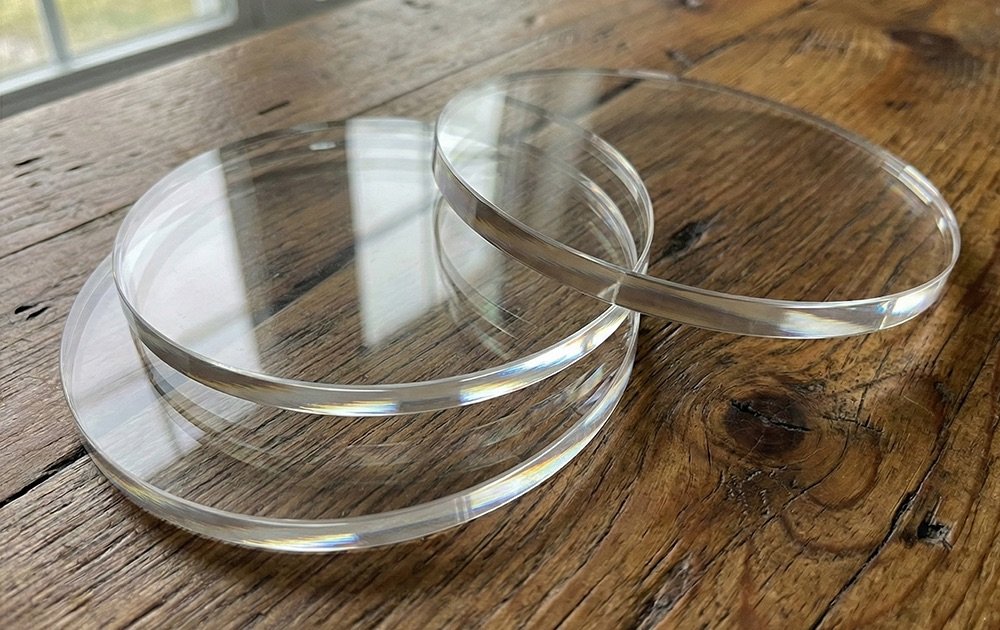
Materials engineering continues to push boundaries across electronics, telecommunications, and optics, driving demand for specialized substrates that can withstand harsh conditions while delivering unmatched performance. Among these materials, silicon dioxide in its crystalline and fused forms plays a foundational role. At the heart of many high-precision applications is the quartz wafer, a specialized disc engineered from either naturally occurring or synthetically grown quartz crystals. These components serve as critical platforms for devices ranging from advanced semiconductor components to high-frequency oscillators and precision optical lenses.
Natural versus Synthetic Quartz Growth
Quartz forms naturally in prismatic crystal structures deep within the earth, but the rigorous demands of modern technology require a more controlled approach. Engineered or cultured quartz is grown in large, artificial hydrothermal autoclaves under extreme pressure and temperature conditions. This synthetic process allows manufacturers to produce ultra-pure silicon dioxide blocks with minimal defects, controlled lattice structures, and precise impurity levels. Once harvested, these large crystals are carefully inspected, oriented along specific crystallographic axes, and sliced into individual units. The resulting quartz wafer provides a reliable, uniform foundation that natural quartz rocks simply cannot guarantee at a mass-manufacturing scale. Furthermore, fused quartz—derived from melting high-purity silica—offers an amorphous alternative that lacks a long-range crystalline order, yet delivers distinct optical and thermal advantages.
Core Material Properties of a Quartz Wafer
The versatility of a quartz wafer stems directly from its exceptional physical, chemical, and electrical characteristics. Unlike standard silicon or standard glass substrates, quartz exhibits a unique combination of properties that make it indispensable in extreme environments. Engineers and designers often turn to these components when standard materials fail under thermal stress, chemical exposure, or electromagnetic interference.
Thermal and Chemical Resistance
One of the most defining characteristics of any high-quality quartz wafer is its incredible resistance to heat and thermal shock. Fused and single-crystal quartz possess exceptionally high softening and melting points, often exceeding 1600 degrees Celsius, alongside a remarkably low coefficient of thermal expansion. This means that a quartz wafer can undergo rapid and extreme temperature fluctuations without cracking, warping, or degrading. Additionally, the material is chemically inert to most acids, bases, and organic solvents, save for hydrofluoric acid. This chemical stability ensures that processing chemicals do not leach impurities into the substrate or react adversely during delicate manufacturing procedures.
Optical Clarity and Electromagnetic Performance
Beyond thermal durability, a quartz wafer offers stellar optical transmission properties across a broad spectrum ranging from deep ultraviolet (UV) through the visible light spectrum and well into the infrared (IR) range. This broad optical window makes it a preferred medium for specialized optical components, laser systems, and viewports. Electrically, quartz is an outstanding electrical insulator with a low dielectric constant and minimal loss tangent. These characteristics enable a quartz wafer to manage high-frequency radio signals efficiently, making it an ideal substrate for high-frequency telecommunication components and radio frequency filters.
Manufacturing and Precision Slicing Techniques
Transforming a raw synthetic quartz boule into a finished, polished quartz wafer requires sophisticated machinery, meticulous planning, and precise geometric control. Because quartz is a hard material with a Mohs hardness rating of 7, standard cutting techniques are insufficient. Manufacturers employ advanced wire saws embedded with diamond grit or high-precision laser ablation systems to slice the crystal boules into thin, uniform disks without introducing severe mechanical stress or micro-fractures.
Crystal Orientation and Orientation Cuts
The performance of single-crystal components depends heavily on how the slice is oriented relative to the crystal’s natural axes. Depending on the intended end-use, a quartz wafer can be fabricated using various specialized cuts. For instance, Z-cut wafers are frequently utilized for optical applications and basic substrates, whereas AT-cut and BT-cut slices—oriented at precise angles relative to the optical Z-axis—are legendary for their superior frequency stability across changing temperatures. These specialized orientation cuts ensure that the resulting devices maintain optimal resonance and minimal drift over time.
Surface Polishing and Finishes
Once sliced, the raw wafers undergo intensive lapping, grinding, and polishing steps to achieve the desired thickness, flatness, and surface roughness. Surface finishes can range from ultra-smooth, mirror-like optical polishes with root-mean-square roughness values of less than a nanometer to fine-ground or etched textures depending on the application requirements. Total thickness variation and bow are kept to strict tolerances to ensure that downstream processing steps, such as photolithography or thin-film deposition, proceed without alignment errors or surface irregularities.
Major Industrial Applications
The unique intersection of mechanical strength, optical transparency, and piezoelectric behavior enables the quartz wafer to serve a vast array of high-tech industries. From computing infrastructure to aerospace instrumentation, these specialized disks play a silent yet vital role in everyday modern life.
Semiconductor Fabrication and Photolithography
In the semiconductor industry, quartz plays a dual role. While single-crystal components are used for specific frequency-control elements, fused varieties of the quartz wafer are heavily relied upon in photolithography. Because semiconductor manufacturing relies on extreme ultraviolet and deep ultraviolet light to pattern microchips onto silicon substrates, the photomasks must be built on a material that does not distort under light exposure or thermal load. Quartz provides the ultimate optical transparency and dimensional stability required for producing faultless photomasks. Furthermore, high-purity quartzware, including carrier boats and tubes, is used extensively in high-temperature diffusion, oxidation, and chemical vapor deposition furnaces.
Piezoelectric Devices and MEMS Sensors
One of the most profound physical properties of single-crystal quartz is its piezoelectricity—the ability to generate an electrical charge in response to applied mechanical stress, and vice versa. This direct electromechanical coupling allows a quartz wafer to act as the fundamental building block for precision timing devices, quartz crystal microbalances, and frequency resonators. In modern microelectromechanical systems (MEMS), quartz-based accelerometers, pressure sensors, and gyroscopes utilize this phenomenon to measure physical forces with extreme accuracy, making them critical components in aerospace navigation, automotive safety systems, and industrial monitoring equipment.
Optics, Photonics, and Telecommunications
The broad spectral transmission of a quartz wafer also makes it indispensable in advanced photonics and laser technology. It serves as an ideal substrate for optical wave plates, polarizers, prisms, and lens systems used in high-power laser environments where standard glasses would quickly degrade or absorb too much energy. In telecommunications, quartz components help route optical signals through fiber-optic networks with minimal attenuation and signal degradation, ensuring high-speed global connectivity.
Future Trends and Market Outlook
As emerging technologies demand higher efficiency, miniaturization, and operation in increasingly extreme environments, the demand for precision components continues to surge. Trends toward glass-free cleanrooms, higher frequency wireless communications, and advanced quantum computing architectures are driving manufacturers to refine fabrication processes even further. Innovations in laser slicing, automated surface inspection, and ultra-thin wafer production are reducing costs while pushing performance limits higher. The ongoing evolution of the quartz wafer ensures that it will remain an irreplaceable cornerstone of advanced engineering, bridging the gap between raw geological wonders and the pinnacle of modern technological achievement.